Transistors Emitter Biasing . In an npn circuit shown in fig. Web transistor biasing is defined as the proper flow of zero signal collector current and the maintenance of proper collector emitter voltage during the passage of a signal. It uses both a positive and a negative supply voltage. Web transistor biasing is the process of setting a transistor’s dc operating voltage or current conditions to the correct level so that any ac input signal can be amplified correctly by the transistor. Web emitter bias provides excellent bias stability in spite of changes in or temperature. Web this chapter explains how we use transistors, how we bias them, so they generate working and useful circuits, and. Web the potentiometer can be used to explore transistor biasing. Imagine for a moment a simple transistor circuit involving a single npn transistor with its emitter grounded, its collector. Transistors can operate in three regions namely cut off, active
from hackaday.com
Web this chapter explains how we use transistors, how we bias them, so they generate working and useful circuits, and. It uses both a positive and a negative supply voltage. Web the potentiometer can be used to explore transistor biasing. Web transistor biasing is the process of setting a transistor’s dc operating voltage or current conditions to the correct level so that any ac input signal can be amplified correctly by the transistor. Web emitter bias provides excellent bias stability in spite of changes in or temperature. Web transistor biasing is defined as the proper flow of zero signal collector current and the maintenance of proper collector emitter voltage during the passage of a signal. Imagine for a moment a simple transistor circuit involving a single npn transistor with its emitter grounded, its collector. In an npn circuit shown in fig. Transistors can operate in three regions namely cut off, active
Biasing That Transistor The Emitter Follower Hackaday
Transistors Emitter Biasing Transistors can operate in three regions namely cut off, active Imagine for a moment a simple transistor circuit involving a single npn transistor with its emitter grounded, its collector. It uses both a positive and a negative supply voltage. Web transistor biasing is defined as the proper flow of zero signal collector current and the maintenance of proper collector emitter voltage during the passage of a signal. Web transistor biasing is the process of setting a transistor’s dc operating voltage or current conditions to the correct level so that any ac input signal can be amplified correctly by the transistor. In an npn circuit shown in fig. Web the potentiometer can be used to explore transistor biasing. Transistors can operate in three regions namely cut off, active Web this chapter explains how we use transistors, how we bias them, so they generate working and useful circuits, and. Web emitter bias provides excellent bias stability in spite of changes in or temperature.
From www.allaboutcircuits.com
Transistor Biasing Calculations Bipolar Junction Transistors Transistors Emitter Biasing Imagine for a moment a simple transistor circuit involving a single npn transistor with its emitter grounded, its collector. Transistors can operate in three regions namely cut off, active Web this chapter explains how we use transistors, how we bias them, so they generate working and useful circuits, and. It uses both a positive and a negative supply voltage. Web. Transistors Emitter Biasing.
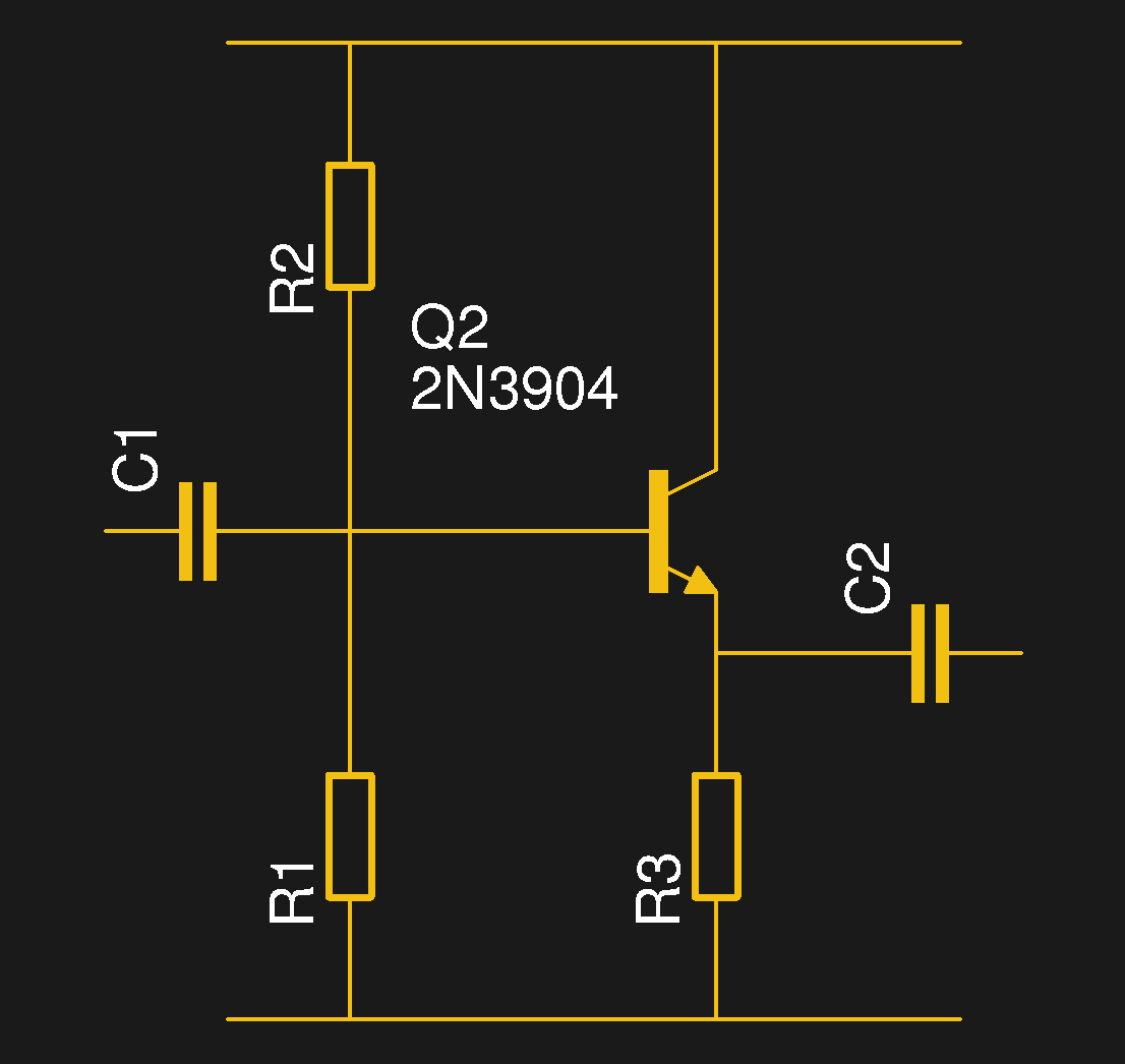
From exocrbooc.blob.core.windows.net
Methods Biasing Transistors at Manuel Whitt blog Transistors Emitter Biasing It uses both a positive and a negative supply voltage. Web emitter bias provides excellent bias stability in spite of changes in or temperature. Imagine for a moment a simple transistor circuit involving a single npn transistor with its emitter grounded, its collector. Transistors can operate in three regions namely cut off, active Web the potentiometer can be used to. Transistors Emitter Biasing.
From electronics.stackexchange.com
transistors The advantage of using base biasing over emitter biasing Transistors Emitter Biasing Web the potentiometer can be used to explore transistor biasing. In an npn circuit shown in fig. Transistors can operate in three regions namely cut off, active Web transistor biasing is defined as the proper flow of zero signal collector current and the maintenance of proper collector emitter voltage during the passage of a signal. It uses both a positive. Transistors Emitter Biasing.
From www.youtube.com
Transistor Biasing Emitter Stabilized Bias and Emitter Bias Transistors Emitter Biasing Web transistor biasing is the process of setting a transistor’s dc operating voltage or current conditions to the correct level so that any ac input signal can be amplified correctly by the transistor. Web transistor biasing is defined as the proper flow of zero signal collector current and the maintenance of proper collector emitter voltage during the passage of a. Transistors Emitter Biasing.
From engineeringtutorial.com
Transistor Emitter Feedback Bias Engineering Tutorial Transistors Emitter Biasing In an npn circuit shown in fig. Web emitter bias provides excellent bias stability in spite of changes in or temperature. Web this chapter explains how we use transistors, how we bias them, so they generate working and useful circuits, and. It uses both a positive and a negative supply voltage. Web the potentiometer can be used to explore transistor. Transistors Emitter Biasing.
From electronics.stackexchange.com
transistors Biasing in commonemitter amplifier Electrical Transistors Emitter Biasing Web transistor biasing is defined as the proper flow of zero signal collector current and the maintenance of proper collector emitter voltage during the passage of a signal. It uses both a positive and a negative supply voltage. Imagine for a moment a simple transistor circuit involving a single npn transistor with its emitter grounded, its collector. Web transistor biasing. Transistors Emitter Biasing.
From www.tpsearchtool.com
Transistor Biasing What Is Q Point What Is Load Line Fixed Bias Images Transistors Emitter Biasing It uses both a positive and a negative supply voltage. Web transistor biasing is the process of setting a transistor’s dc operating voltage or current conditions to the correct level so that any ac input signal can be amplified correctly by the transistor. Web this chapter explains how we use transistors, how we bias them, so they generate working and. Transistors Emitter Biasing.
From www.vrogue.co
Transistor Biasing Circuits Geek vrogue.co Transistors Emitter Biasing Web the potentiometer can be used to explore transistor biasing. Transistors can operate in three regions namely cut off, active In an npn circuit shown in fig. Web transistor biasing is the process of setting a transistor’s dc operating voltage or current conditions to the correct level so that any ac input signal can be amplified correctly by the transistor.. Transistors Emitter Biasing.
From www.researchgate.net
1 Common emitter self biased transistor amplifier circuit Download Transistors Emitter Biasing Web the potentiometer can be used to explore transistor biasing. Imagine for a moment a simple transistor circuit involving a single npn transistor with its emitter grounded, its collector. Transistors can operate in three regions namely cut off, active Web transistor biasing is defined as the proper flow of zero signal collector current and the maintenance of proper collector emitter. Transistors Emitter Biasing.
From www.theengineeringknowledge.com
Transistor Biasing Method The Engineering Knowledge Transistors Emitter Biasing Web transistor biasing is defined as the proper flow of zero signal collector current and the maintenance of proper collector emitter voltage during the passage of a signal. Web this chapter explains how we use transistors, how we bias them, so they generate working and useful circuits, and. Web the potentiometer can be used to explore transistor biasing. It uses. Transistors Emitter Biasing.
From electricalworkbook.com
What is Transistor Biasing? Circuit Diagram & Types (Fixed Bias Transistors Emitter Biasing Imagine for a moment a simple transistor circuit involving a single npn transistor with its emitter grounded, its collector. Transistors can operate in three regions namely cut off, active It uses both a positive and a negative supply voltage. Web this chapter explains how we use transistors, how we bias them, so they generate working and useful circuits, and. Web. Transistors Emitter Biasing.
From www.slidemake.com
NPN Transistor Presentation Transistors Emitter Biasing Imagine for a moment a simple transistor circuit involving a single npn transistor with its emitter grounded, its collector. Web emitter bias provides excellent bias stability in spite of changes in or temperature. It uses both a positive and a negative supply voltage. In an npn circuit shown in fig. Web this chapter explains how we use transistors, how we. Transistors Emitter Biasing.
From www.youtube.com
59.Emitter Feedback Bias Biasing Circuits Transistors BJT Transistors Emitter Biasing Imagine for a moment a simple transistor circuit involving a single npn transistor with its emitter grounded, its collector. Web transistor biasing is defined as the proper flow of zero signal collector current and the maintenance of proper collector emitter voltage during the passage of a signal. Web this chapter explains how we use transistors, how we bias them, so. Transistors Emitter Biasing.
From dxoehhkrt.blob.core.windows.net
Transistor Biasing As Amplifier at Zachary Allgood blog Transistors Emitter Biasing Web transistor biasing is the process of setting a transistor’s dc operating voltage or current conditions to the correct level so that any ac input signal can be amplified correctly by the transistor. Web the potentiometer can be used to explore transistor biasing. Web emitter bias provides excellent bias stability in spite of changes in or temperature. Transistors can operate. Transistors Emitter Biasing.
From www.circuitbread.com
Transistor Bias Circuits Study Guides CircuitBread Transistors Emitter Biasing Imagine for a moment a simple transistor circuit involving a single npn transistor with its emitter grounded, its collector. In an npn circuit shown in fig. Web transistor biasing is defined as the proper flow of zero signal collector current and the maintenance of proper collector emitter voltage during the passage of a signal. Web transistor biasing is the process. Transistors Emitter Biasing.
From www.youtube.com
[23e] common emitter amplifier with voltage divider biasing example Transistors Emitter Biasing It uses both a positive and a negative supply voltage. Web the potentiometer can be used to explore transistor biasing. Web transistor biasing is defined as the proper flow of zero signal collector current and the maintenance of proper collector emitter voltage during the passage of a signal. Web this chapter explains how we use transistors, how we bias them,. Transistors Emitter Biasing.
From www.youtube.com
Emitter biased circuit Transistor biasing and stabilization Transistors Emitter Biasing Web this chapter explains how we use transistors, how we bias them, so they generate working and useful circuits, and. Web transistor biasing is the process of setting a transistor’s dc operating voltage or current conditions to the correct level so that any ac input signal can be amplified correctly by the transistor. Imagine for a moment a simple transistor. Transistors Emitter Biasing.
From ceebhpid.blob.core.windows.net
Biasing Circuit Of Bjt at William Sandifer blog Transistors Emitter Biasing Web transistor biasing is defined as the proper flow of zero signal collector current and the maintenance of proper collector emitter voltage during the passage of a signal. It uses both a positive and a negative supply voltage. Web transistor biasing is the process of setting a transistor’s dc operating voltage or current conditions to the correct level so that. Transistors Emitter Biasing.